
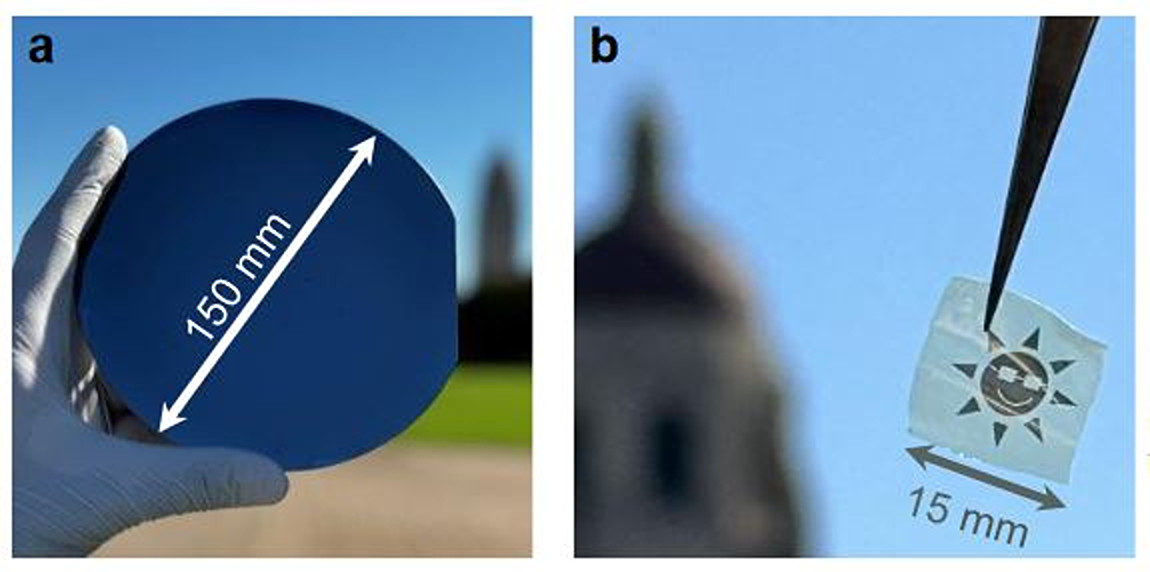
The group designed a sputtered multilayer WSe2 film with a thickness of 15−30 nm for applications on on a 150 mm wafer via a selenization process based on either a solid-source selenium (SS-Se) at 900 C or low-thermal-budget hydrogen selenied (H2Se) precursors at 650 C. The resulting WSe2 film had an energy bandgap of 1.2 eV to 1.3 eV, which the scientists described as near-ideal for solar energy harvesting.
Yep. Those are words
Are they?
The words definitely are. I have no idea what the initialisms are though.
Jokes aside: those are chemical compounds, mostly based on Selenium (Se).
Of all the words in the world, those are certainly some of them