- cross-posted to:
- hardware@lemmy.world
- cross-posted to:
- hardware@lemmy.world
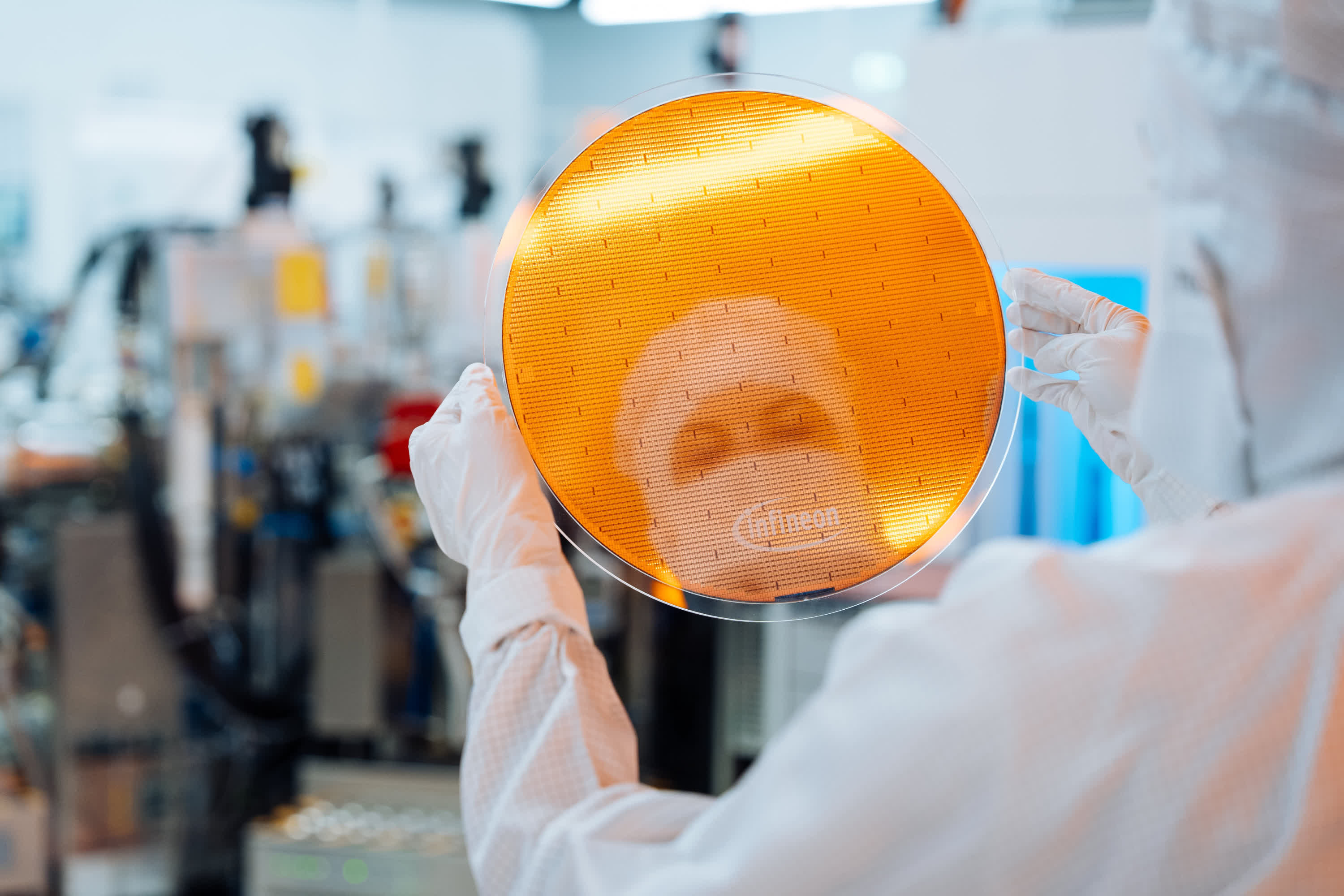
The thinness of silicon wafers is important because it reduces resistance and power loss. Current-gen wafers measure 40 to 60 micrometers thick. By roughly halving the wafer’s thickness, Infineon has managed to slash substrate resistance by 50 percent. This, in turn, leads to over 15 percent less power loss compared to other solutions.
You must log in or register to comment.


